
Revision summary
India designs many chips but still makes few, because fabs need capital, ultra-pure water, chemicals and restricted tools. Geopolitics and long project time add risk. The India Semiconductor Mission (2021) has about ₹76,000 crore for fabs, display, compound semiconductors and packaging. A design-linked incentive targets the talent India already has. Mature nodes and ATMP are the realistic near path; leading-edge logic will follow slowly if at all.
Model answer
Copper italics in this answer — like this — are the key facts. Each one is unpacked in the Facts & figures rail.
Introduction
Semiconductor ambition and India
Semiconductors are foundational to modern electronics, defence, automobiles and digital infrastructure. India has strong capabilities in chip design and engineering talent, but limited domestic fabrication and a fragmented manufacturing ecosystem. The India Semiconductor Mission (ISM) seeks to bridge these gaps and build a resilient semiconductor ecosystem.
Body
Challenges faced by India's semiconductor industry
- Limited fabrication ecosystem: India has strong chip-design capabilities but historically lacked commercial-scale semiconductor fabs, limiting domestic manufacturing.
- Example: India's strength in semiconductor design has not been matched by a comparable domestic wafer-fabrication ecosystem.
- High capital and infrastructure requirements: Semiconductor fabrication requires very high investment, uninterrupted electricity and large quantities of ultra-pure water. Even small disruptions can cause significant production losses.
- Example: A fabrication plant requires continuous power and ultra-pure water for wafer-cleaning and manufacturing processes.
- Concentrated global ecosystem: Semiconductor manufacturing is dominated by a few countries and firms, particularly Taiwan and South Korea, creating high entry barriers for India.
- Example: India's entry into fabrication requires competing with established global semiconductor manufacturing clusters.
- Skill and talent gap: India has a large engineering workforce, but advanced semiconductor manufacturing requires specialised skills in fabrication, process engineering, packaging and equipment.
- Example: Engineering talent needs specialised industry-oriented training for semiconductor fabrication and process engineering.
- Weak R&D ecosystem: Limited domestic original semiconductor research and technology development constrain India's ability to move beyond design and assembly.
- Example: Strengthening institutions such as the Semiconductor Laboratory (SCL), Mohali is important for building domestic capabilities.
- Complex clearances: Semiconductor fabs require multiple technological, environmental and governmental clearances, increasing project complexity and gestation periods.
- Example: Large semiconductor projects must coordinate technological requirements with multiple regulatory approvals.
- Import-dependent supply chain: Critical equipment, chemicals, components and technologies remain dependent on imports, exposing the industry to geopolitical and supply-chain disruptions.
- Example: Dependence on specialised imported equipment and inputs can affect production when global trade or geopolitical conditions change.
Salient features of the India Semiconductor Mission
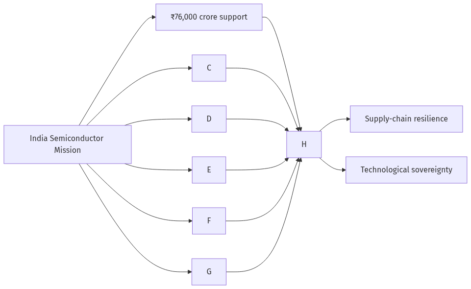
- ₹76,000 crore financial support: The Semicon India Programme provides substantial fiscal support for developing semiconductor and display manufacturing capabilities.
- Example: The programme supports the development of semiconductor and display fabrication capacity in India.
- Support across the value chain: ISM supports semiconductor fabs, display fabs, compound semiconductors and ATMP/OSAT facilities, rather than focusing only on wafer fabrication.
- Example: ATMP/OSAT facilities strengthen the downstream assembly, testing and packaging segment of the semiconductor value chain.
- Design support: The mission includes a Design Linked Incentive (DLI) to support domestic semiconductor design companies and strengthen India's existing design capability.
- Example: DLI helps India leverage its existing strength in chip design while expanding domestic semiconductor capabilities.
- Compound semiconductor ecosystem: Support for compound semiconductors such as SiC and GaN helps develop capabilities relevant to EVs, power electronics and telecommunications.
- Example: SiC and GaN are important for power electronics and advanced telecommunications applications.
- Attracting global investment and technology: 100% FDI under the automatic route in electronics and semiconductor manufacturing helps attract global capital, technology and expertise.
- Example: Global investment can bring capital, technical expertise and manufacturing know-how into India's semiconductor ecosystem.
- Domestic manufacturing ecosystem: ISM aims to develop an integrated ecosystem covering fabrication, packaging, testing, design and associated supply chains, thereby improving technological sovereignty and supply-chain resilience.
- Example: Developing fabs alongside ATMP/OSAT and design capabilities reduces dependence on a fragmented external supply chain.
- Strategic partnerships: India is pursuing international cooperation, including the Quad Semiconductor Supply Chain Initiative, to diversify supply chains and strengthen technological partnerships.
- Example: Cooperation with Australia, Japan and the United States can help strengthen and diversify semiconductor supply chains.
Flow diagram
Conclusion
India's semiconductor ambitions are constrained by capital intensity, infrastructure requirements, specialised skills, weak fabrication capabilities and import dependence. The India Semiconductor Mission addresses these constraints through ₹76,000 crore support, fab and packaging incentives, design support, compound-semiconductor development and global partnerships, providing the foundation for a resilient domestic semiconductor ecosystem.
Quick related
Students also ask
-
Why is maritime security vital to protect India's sea trade? Discuss maritime and coastal security challenges and the way forward.
Next question on this syllabus topic (2025 · Q20). View answer →
-
Can India copy Taiwan in five years?
No. Taiwan’s cluster is two generations of firms and skills. India can win packaging and mature nodes first.
-
Why subsidise chips at all?
Because security and electronics imports are strategic, and private capital will not build a first fab unaided.
Same topic · past papers
UPSC has asked this before
These previous-year questions sit on the same topic. Open one to practise the earlier ask.
-
2026 · Q15 · GS III · 15 marks
Mention salient features of 'Mission Drishti'. Discuss the imaging techniques used in the satellite launched on 3rd May 2026. Why is it being considered world's first satellite of its kind? -
2026 · Q17 · GS III · 15 marks
What are the challenges to solid waste management in India? Discuss the governmental policy framework on solid waste management. Discuss the success/failure cases of Delhi and Indore cities highlighting the salient features of their solid waste management initiatives. -
2016 · Q13 · GS III · 12 marks
Why is nanotechnology one of the key technologies of the 21st century? Describe the salient features of Indian Government's Mission on Nanoscience and Technology and the scope of its application in the development process of the country. -
2026 · Q9 · GS III · 10 marks
Explain how fake news and disinformation pose threat to Internal Security and Public Order in Indian context? In this regard, discuss salient features of amendments in respect of Information Technology (Intermediatory Guidelines and Digital Media Ethics Code) Rules 2021. -
2024 · Q13 · GS III · 15 marks
What are the major challenges faced by Indian irrigation system in recent times? State the measures taken by the government for efficient irrigation management.
More from this topic
Q17 · UPSC Mains 2026 · GS III · 15 marks · Solution
What are the challenges to solid waste management in India? Discuss the governmental policy framework on solid waste management. Discuss the success/failure cases of Delhi and Indore cities highlighting the salient features of their solid waste management initiatives.
Indian Economy
• Rapid urbanization has made solid waste management a critical environmental and public health crisis in India. • Key challenges include lack of source segregation, inadequate processing infrastructure, reliance on unprotected informal workers, and financially weak urban local bodies. • The policy framework relies on the SWM Rules 2016, Swachh Bharat Mission (Urban), and Plastic Waste Management Rules 2016. • Indore succeeded through 100% source segregation, zero dump-site remediation, and strict enforcement with digital monitoring. • Delhi failed due to overloaded legacy landfills (Ghazipur, Bhalswa), lack of decentralization, and fragmented municipal governance. • A successful transition requires moving to a circular economy focused on source segregation, decentralized processing, and polluter accountability.
Q16 · UPSC Mains 2026 · GS III · 15 marks · Solution
What is Agentic Artificial Intelligence (AI)? Explain its working. Describe its applications with suitable examples. Discuss the advantages, risks and challenges associated with agentic AI systems.
Indian Economy
Agentic Artificial Intelligence represents an advanced paradigm where AI systems operate with autonomy, setting goals and executing complex workflows without constant human prompts. Unlike traditional generative AI that merely responds to queries, agentic AI uses perception, planning, memory, and tool-use to achieve multi-step objectives. Its applications span across autonomous software engineering, supply chain optimization, and automated financial trading. While offering massive productivity gains and dynamic problem-solving, these systems pose significant risks including lack of transparency, alignment failures, security vulnerabilities, and ethical dilemmas. Governance frameworks and robust guardrails are essential to harness their potential safely.
Q15 · UPSC Mains 2026 · GS III · 15 marks · Solution
Mention salient features of 'Mission Drishti'. Discuss the imaging techniques used in the satellite launched on 3rd May 2026. Why is it being considered world's first satellite of its kind?
Indian Economy
Mission Drishti represents a major leap in India's space-based Earth observation capabilities, launched on 3rd May 2026. The mission employs advanced multi-spectral and hyperspectral imaging techniques to capture high-resolution data across various atmospheric and terrestrial layers. It is hailed as a global first due to its unique integration of real-time onboard edge computing with quantum encryption for secure data transmission. The satellite significantly enhances resource management, disaster response, and strategic surveillance. It aligns with India's policy of leveraging space technology for sustainable development and national security.